The Printed Circuit Board
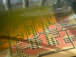
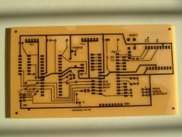
I use Seno etch-resist transfers to make my printed circuit boards so their layouts tend to be relatively simple with very little complicated track routing. Once I'm happy with the layout, I scan the copper side of the board and print out a full size image. I can then double-check that everything will fit by laying the actual components on the paper copy.
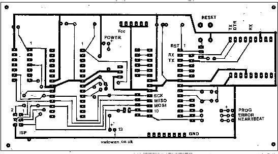
Some circuit errors or component placing errors generally show up at this stage. With a bit of colour manipulation in PaintShop Pro, the result is the image you see above - a direct scan of the actual PCB. The component-side layout is simply made by selecting "Mirror" from the PaintShop Pro menu and then adding the component overlay.
 |  |
 |
Once I'm happy with the layout, it's just a case of leaving the board, copper side up, in the ferric chloride etching solution until all the unprotected copper is etched away. The board is then washed under running water and the etch resist removed. I use a kitchen sponge (the type with a nylon scouring side) for that job. After it's dried, the holes can be drilled. I find a 0.7 or 0.8 mm drill bit about right for most components.
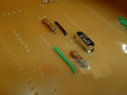
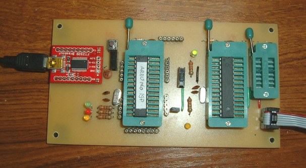
Insert and solder the components in the "usual order" - ie, start with those that are flattest to the board (the 5 wire links), then the resistors and the two 16MHz crystals, and so on. And here's the finished board, powered up, LEDs blinking...!
So..... on to the programming!