Construction
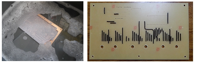 I used the laser printer & hot iron method to etch the single-sided PCB so there are a lot of links to solder. In the absence of
professional through-hole plating facilities, a home-manufactured double-sided PCB would have resulted in twice as many solder joints and, I think,
would have looked a mess!
I used the laser printer & hot iron method to etch the single-sided PCB so there are a lot of links to solder. In the absence of
professional through-hole plating facilities, a home-manufactured double-sided PCB would have resulted in twice as many solder joints and, I think,
would have looked a mess!
As with any PCB, start with the lowest profile parts first - in this case the wire links - so the board will lie flat when you turn it over to solder.
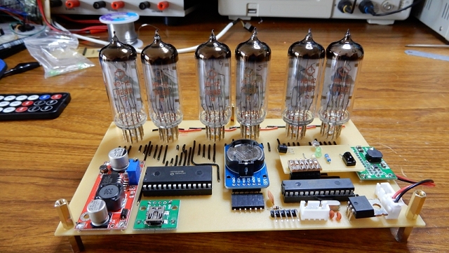
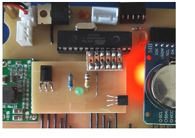
 This photo shows the sockets for the ATmega328P and the HV5812P-G soldered in place. Also, the 10k reset pull-up resistor, the 16MHz crystal and two 22pF capacitors for the ATmega328P.
The green module is a breakout board for a mini-USB socket for the 5 volt power input.
The blue DC-DC converter was later replaced with one with a higher voltage output.
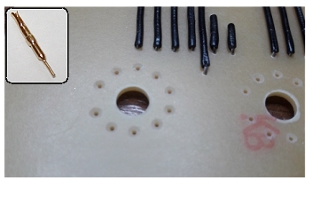 This photo shows a close-up of the holes for the IV-12 tube base pins. Unfortunately, conventional tube bases are not available for the IV-12 so individual pins are used (see inset).
I found the best way to insert the pins into the PCB, and ensure they were correctly aligned, was to fit them to the IV-12 tube bases first and 'jiggle' the combined pins and tube into the PCB holes. It's very fiddly so I countersunk the PCB holes slightly to make it slightly easier to align the pins with the holes.
For the tubes to stand at the correct height above the PCB, only the narrow end of the pin is inserted. The diameter of the narrow section is 0.6mm.
However, I recommend that you leave the pins & tubes safely to one side at this stage. It is safer to do some voltage checks on the rest of the board before the tube pins are soldered into place.
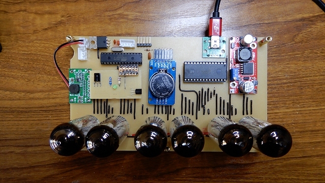
 I mounted the TSOP38238 IR receiver, the TMP36 temperature sensor and the "Alarm Set" LED on a small "daughter board"
which plugs into a pin header on the main PCB adjacent to the ATmega328P.
I mounted the TSOP38238 IR receiver, the TMP36 temperature sensor and the "Alarm Set" LED on a small "daughter board"
which plugs into a pin header on the main PCB adjacent to the ATmega328P.
The daughter board also picks up 5v (Vcc) and ground.
How/where you mount these sensors is personal choice and depends on the sort of enclosure you envisage for the finished clock.
I used semi-transparent grey acrylic (Perspex type 923) for the top of my enclosure and found that the IR sensor worked fine through it. The "Alarm Set"
LED would be better mounted in a more visible position and the TMP36 temperature sensor might be better mounted externally but the complete daughter board does enable the whole clock to be tested. The positioning of various items can be fine tuned later. LDR sits behind a hole in the front of the enclosure with flying leads to the daughter board.
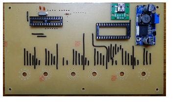
 Solder the rest of the componenents in place except the IV-12 tubes/pins. Solder the two DC-DC converters in place.
Don't insert the ATmega328P or the HV5812P-G at this stage.
Connect 5 volts to the 5v input mini USB socket and measure 5 volts on the correct pins on the ATmega328P socket and pin 28 on the HV5812P-G socket.
Measure the voltage on pin 1 on the HV5812P-G socket and adjust the 50v DC-DC boost converter for about 25 volts (for now). The volatge can be increased later.
Bridge the "1.5v" solder link on the 1.5v buck converter and check for 1.5v at its output and, ideally, across the solder pads for pins 2 and 3 of each IV-12.
If you're going to use an external programming lead such as this one, insert an ATmega328P (with a bootloader) into its socket. Alternatively, program the ATmega328P externally and then insert it into its socket. Insert the HV5812P-G into its socket.
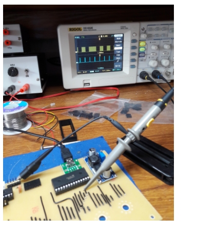
You can use a 'scope at this point to check for some activity on the data pin on the HV5812P-G and on some of its output pins. At this stage, you should see around a 25v square wave at the outputs.
With everything powered down, it's time to solder in the 60 tube pins. As I mentioned earlier, to make sure the pins were aligned vertically and that all the tubes were level horizontally, I soldered in the pins complete with their IV-12 tubes. It's a very fiddly job but, once it's done, it's done.