Laying out the components
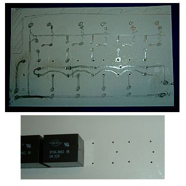
Begin by cutting a piece of paper or thin card and laying out the components whilst
trying to connect their pins according to the circuit. Remember that the connecting lines
can't cross one another but, by using a pencil and paper in this way, you can try many
different layouts until you're happy with the result.
For a simple circuit such as this, the layout isn't at all critical and the drawing doesn't have to be particularly neat. Where the spacing between the pins on a component is critical (such as the miniature relays), you can use the component itself to mark the positions by laying it on the paper or card and pressing gently. The marks can then be pierced through the card with a darning needle (Bottom photograph).
Once you're happy with the layout and you've double checked that the inter-connections correspond with the circuit diagram, you're ready to prepare the printed circuit board and transfer the design to it.