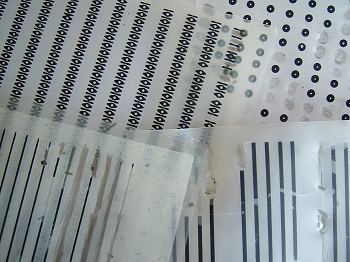
The etch-resist transfers
There are several methods of making the printed circuit board resistant to the etching process. One popular method uses board which is pre-coated with a coating sensitive to UV light. The track layout is printed onto acetate film which is used, in effect, as a negative to make a contact 'print' on the copper. Parts of the copper which where exposed to UV light become soluble in the etchant.Another modern method requires the use of a laser printer or photo-copier to produce the track layout on special "press n peel" film. This is then ironed onto the copper printed circuit board. When it is peeled off, the etch-resistant tracks remain on the board.
The simplest method of all consists simply of a felt tip pen containing special etch-resistant ink. These pens are good to 'touch up' parts of a board prior to etching but I wouldn't recommend them for making the entire board.
|
|
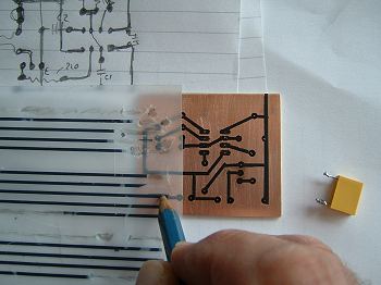
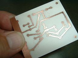
| We're going to use etch-resist transfers as shown here. They come on sheets of clear acetate and are simply transferred to the printed circuit board by rubbing with a blunt, hard pencil. | With your piece of printed circuit board clean and shiny, copy the layout from your pencil drawing as shown above. Once the transfers are in place, cover them with a sheet of the transfer's backing paper and press down really hard. |
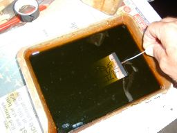
| The etch-resist solutionWhen the board is complete, give it a final, thorough check-over. Make sure the tracks and pads are thoroughly pressed onto the copper and there are no errors in the layout.Mix the etching solution as per the instructions and pour it carefully into an old plastic dish. I use an old photographic developer dish. Treat this solution with care. It is toxic, corrosive and will badly stain anything it comes into contact with. Do not allow it to contact bare skin. Preferrably, use forceps or an old plastic clothes peg to handle the board. |
| Lift the board from the solution at frequent intervals. This will allow fresh
solution onto the surface of the board to assist the etching proccess. With fresh solution, it will take
about 40 minutes to an hour to etch away the unwanted areas of copper. Don't leave the board in the solution longer than necessary or the etching solution will begin to undercut the etch-resist transfers. Conversely, don't remove it too soon or there could be areas of copper not completely etched away where tracks are close together. |
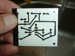
| When you're sure the etching is complete, lift the board from the solution and
rinse it thoroughly with plenty of warm running water. Finally, use washing up liquid and an old kitchen sponge - the type with a scouring surface on one side - to remove the etch-resist and produce a PCB with
clean, shiny copper. Examine it carefully again, using a magnifying glass if necessary, to make sure there are no hairline cracks in the tracks (these can usually be bridged with solder if there are any) and check that any tracks which are close together are not bridged with un-etched copper (use a sharp needle to clear them if there are any such areas). |